

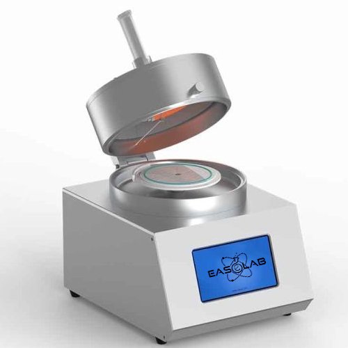
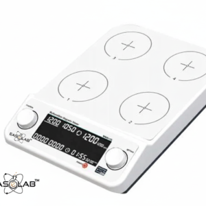
Spin Coater
₹175,000.00
A spin coater, often simply called a “spinner,” is a crucial laboratory instrument used in materials science and engineering to deposit extremely uniform, thin films onto flat substrates.
Description
Model: ELSC-001
| Make | EASELAB |
| Mode | ELCS-001 |
| Speed | 100 – 12000 RPM |
| Acceleration | Up to 6000 RPM/s |
| Standard Chucks | 1 Vacuum Chuck |
| Drainpipe | To be attached on the side of the chamber |
| Housing Material | Corrosion-free Powder Coated Sheet Metal Glove Box Compatible |
| Time per Step | 10000 seconds |
| Display | Semi-Integrated Android based Tablet Controller (Manual ON/OFF) |
| PC Connectivity | YES |
| Graph Display | LIVE RPM vs TIME graph during spinning time |
| Program Steps | 100 steps per program |
| Storage Capacity | Up to 4 GB |
| Substrate Holding Mechanism | Hybrid Vacuum and Vacuum less |
| Substrate Size | 10 mm up to 2 inches – Holder/Chuck Material |
| Working Chamber Material | Natural Polypropylene (PP) – 9 inches |
| Substrate Holding Vacuum | 650 mmhg through oil-free vacuum pump |
| Vacuum Connections | 10 mm PU hose – 2 m length – default |
| Safety Feature | Lid Interlock safety for open cover |
| Liquid Dispensing | Centre Hole in the Lid for liquid dispensing |
| Lid Material | Transparent Acrylic Top lid |
| Nitrogen Purging | Pneumatic connection in the lid for N2 Purging |
| Power | 220 V AC/50 Hz |
Use of Spin Coater:
Here are the primary applications of the spin coater, categorized by industry: Electronics and Semiconductor Manufacturing This is historically the most widespread and critical application of spin coating.
-
Photolithography: The cornerstone of microelectronics. Spin coating is used to apply uniform layers of photo resist (a light-sensitive polymer) onto silicon wafers. This uniform layer is essential for precisely patterning and etching integrated circuits, microprocessors, and memory chips.
-
Insulating and Conductive Layers: Used to deposit thin films of dielectric materials, polymers, and conducting oxides needed for various components within an integrated circuit (IC).
-
Organic Light-Emitting Diodes (OLEDs): Spin coating is a key method for depositing the organic material layers that make up the active and emissive components of flexible and high-resolution displays.
-
Transistors: Used in the fabrication of various thin-film transistors (TFTs) and field-effect transistors (FETs).
Renewable Energy and Optoelectronics The ability to create large-area, uniform coatings makes it ideal for energy harvesting and light-based technologies.
-
Thin-Film Solar Cells (Photovoltaic): Crucial for depositing layers of new materials like Perovskites and various organic semiconductors to create high-efficiency solar cells.
-
Anti-Reflection (AR) Coatings: Used to apply thin, precise polymer or sol-gel layers on lenses, displays, and solar panels to minimise light reflection and maximise light transmission.
-
Optical Data Storage: Used to apply thin, protective, and functional dye layers for optical media (like CDs and DVDs).
Materials Science and Nanotechnology Spin coating is a standard, low-cost method for prototyping and developing novel materials.
-
Polymer Films: Used extensively in research to create thin films of various polymers (like PMMA, PDMS) for studying mechanical, electrical, and optical properties.
-
Nano particle Deposition: Used to assemble thin films from solutions containing metal, metal oxide, or ceramic nano particles (often using the Sol-Gel process).
-
Self-Assembled Monolayers (SAMs): Preparing substrates with organic coatings that self-assemble into highly ordered structures for surface functionalization.
Biomedical and Sensor Technology The precise control over film thickness is vital for devices that interact with biological systems.
-
Biosensors: Used to coat substrates with sensitive materials (polymers, organic materials, bioactive agents) that react to specific biological or chemical species.
-
Drug Delivery Systems: Creating thin, controlled polymer layers for micro- or nano-encapsulation of pharmaceutical agents for controlled release.
-
Bio compatible Coatings: Applying thin layers onto medical devices to improve tissue compatibility or prevent biofouling.
Reviews
There are no reviews yet.